
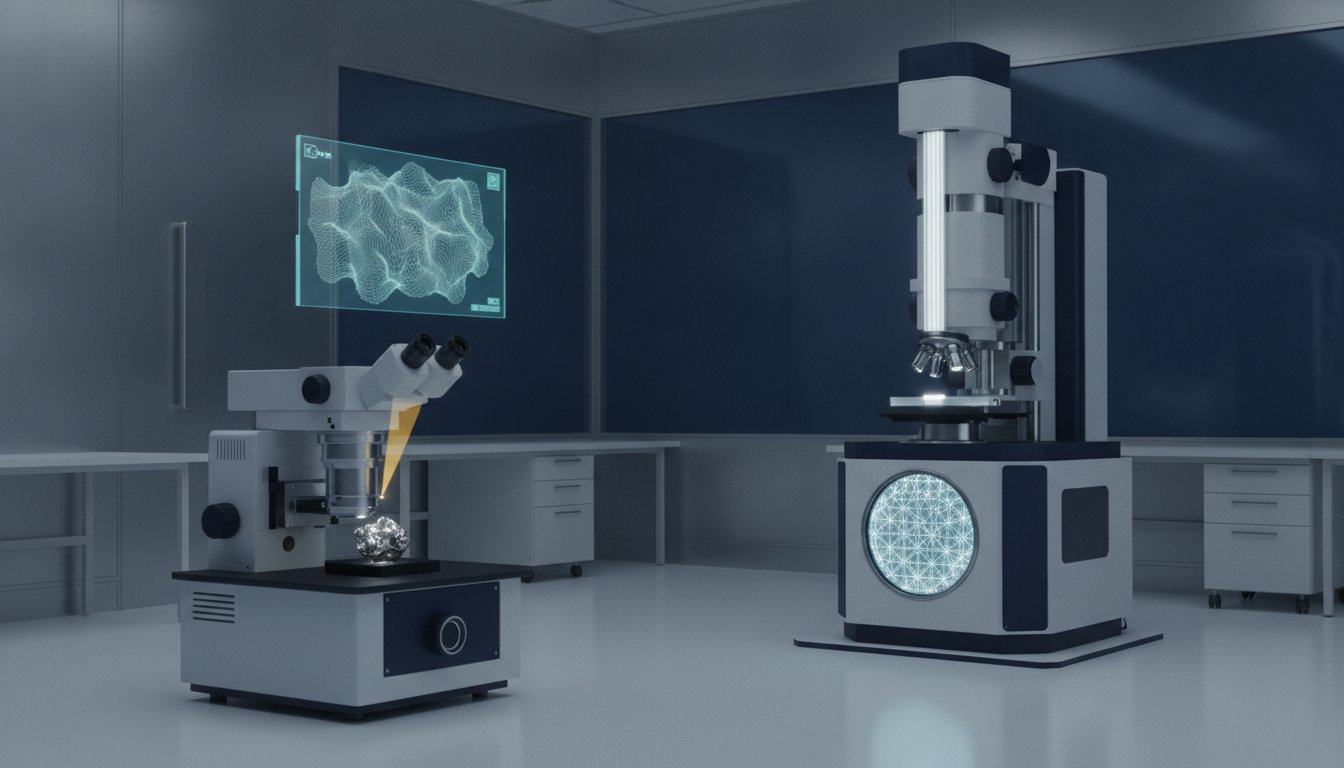
What if the inherent resolution limitations of your current optical systems are the silent inhibitors of your laboratory’s industrial progress? As the global electron microscopy market is projected to reach a valuation of $5.35 billion in 2026, the imperative to distinguish between competing imaging modalities has transitioned from a technical preference to a strategic requirement for global innovators. A precise command of the sem vs tem working principle is essential for any professional seeking to navigate the intricate landscape of electron-matter interactions and signal acquisition. You’re likely aware that the choice between these systems involves more than just a comparison of magnification; it requires a deep understanding of how electron path physics influences the integrity of your analytical data.
This article serves as a technical authority to help you master these operational distinctions and optimize your imaging workflows. We’ll provide a comprehensive analysis of signal generation differences, specifically contrasting the detection of secondary and backscattered electrons with the complexities of transmitted electron paths. You’ll gain a definitive framework for evaluating the versatility of benchtop SEM units, like the Cube II, against the sub-atomic resolution capabilities of floor-model TEM systems. By aligning your hardware selection with the specific requirements of your material analysis, you can ensure that your facility continues to push the boundaries of technical excellence.
Key Takeaways
- Understand the fundamental mechanics of raster scanning and interaction volumes to better utilize secondary and backscattered electron signals for surface topography.
- Analyze the technical distinctions of the sem vs tem working principle to accurately choose between surface-level mapping and internal atomic projection for your specific material analysis.
- Identify the critical role of vacuum dynamics and electromagnetic lens systems in ensuring precise electron trajectory control and preventing beam scattering.
- Learn to evaluate the trade-offs between the sub-atomic resolution of TEM and the high-efficiency, industrial versatility of benchtop SEM systems like the Cube II.
- Develop a strategic framework for justifying laboratory hardware investments based on the required depth of structural data and operational throughput.
The SEM Working Principle: Raster Scanning and Interaction Volumes
The SEM working principle is fundamentally defined by the systematic interaction between a finely focused primary electron beam and the surface of a solid specimen. Unlike other modalities that rely on broad illumination, this process depends on the precise rastering of the beam across a defined area of the sample. This point-by-point interrogation is facilitated by synchronized deflection coils within the column of the electron microscope, which scan the beam in a grid-like rectangular pattern. Essentially, the SEM raster scan acts as the critical mechanism for converting localized electron signals into high-fidelity topographic data, enabling the digital reconstruction of complex surfaces.
A core differentiator in the sem vs tem working principle is the formation of the interaction volume. When the primary beam strikes the specimen, electrons don’t simply reflect off the top layer; they penetrate the material, creating a three-dimensional region of excitation known as the interaction volume. This teardrop-shaped zone is where various signals are generated. The dimensions of this volume are primarily governed by the accelerating voltage, typically measured in kilovolts (kV), and the atomic density of the sample. Higher beam energies lead to deeper penetration, which directly influences the depth from which specific signals, such as characteristic X-rays, originate. Understanding this volume is essential for researchers who must distinguish between true surface features and subsurface data.
Secondary and Backscattered Electrons: The Primary Signals
Secondary electrons (SE) are the result of inelastic scattering and possess low kinetic energy, usually less than 50 eV. Because of this limited energy, only SE generated within the first few nanometers of the surface can escape to the detector, providing the exceptional surface sensitivity required for high-resolution topography and that familiar 3D appearance. Conversely, backscattered electrons (BSE) are high-energy electrons that undergo elastic scattering with the nuclei of the sample atoms. The efficiency of this backscattering is highly dependent on the atomic number (Z), allowing researchers to utilize BSE for material phase identification and compositional contrast. Adjusting the kV allows operators to balance surface detail with subsurface information, a flexibility inherent to the Veritas series and other high-end systems.
Depth of Field and Topographic Contrast
One of the most significant advantages of scanning electron microscopy is its superior depth of field, which far exceeds that of optical systems and transmission-based instruments. This capability arises from the narrow convergence angle of the electron beam as it passes through the final aperture. The resulting images possess a distinctive 3D appearance, largely due to the “shadowing” effect observed in SE detection; surfaces tilted toward the detector appear brighter than those shielded from it. For industrial professionals, mastering SEM operation is vital for optimizing these topographic cues, ensuring that complex geometries are captured with meticulous accuracy and reliable repeatability.
The TEM Working Principle: Electron Transmission and Sub-Atomic Resolution
A definitive technical understanding of the sem vs tem working principle requires acknowledging that TEM is essentially a projection technique. While scanning systems interrogate the surface, the Transmission Electron Microscope (TEM) operates by passing a high-energy electron beam, typically accelerated between 60 kV and 300 kV, directly through an ultra-thin specimen. This interaction allows the electrons to engage with the internal morphology of the sample rather than just its exterior topography. As the beam traverses the material, it undergoes scattering and phase shifts that are subsequently magnified and focused by electromagnetic lenses to produce a 2D projection of the internal structure. This process enables the visualization of features at the sub-nanometer scale, including dislocations, grain boundaries, and even individual atomic columns.
The requirement for specimen transparency is the most significant operational constraint in this modality. To ensure that electrons can successfully exit the sample without undergoing excessive multiple scattering events, specimens must typically be processed to a thickness of less than 100nm. Thicker samples result in a loss of coherence and image clarity, effectively neutralizing the resolution advantages of the system. Beyond standard imaging, the TEM working principle facilitates the capture of electron diffraction patterns. These patterns are critical for determining the crystalline structure and crystallographic orientation of materials at the atomic level, providing data that surface-level scanning cannot replicate. If your laboratory’s objectives prioritize high-throughput surface characterization over internal atomic mapping, integrating a Veritas Series SEM might offer a more streamlined analytical workflow.
Imaging Modes: Bright Field vs. Dark Field
In Bright Field (BF) imaging, the objective aperture is positioned to allow the unscattered electron beam to pass, causing dense or crystalline regions to appear dark against a luminous background. This mode is the standard for observing general morphology and structural defects. Conversely, Dark Field (DF) imaging utilizes only the electrons scattered at specific angles, which highlights particular crystalline phases and lattice orientations with high contrast. Because the de Broglie wavelength of high-energy electrons is exceptionally small, these systems can achieve sub-angstrom resolution, as evidenced by the rigorous standards established in ISO 25387:2026 for point resolution determination.
The Complexity of TEM Sample Preparation
The primary bottleneck in TEM workflows is the rigorous demand for specimen preparation. Achieving the necessary transparency requires specialized techniques such as ultramicrotomy for soft materials or Focused Ion Beam (FIB) milling for hard industrial alloys. These processes are inherently time-consuming and require a high degree of technical meticulousness to avoid introducing artifacts. Consequently, TEM throughput is significantly lower than that of SEM in industrial failure analysis environments. While TEM offers unparalleled depth regarding internal atomic structure, the resource-intensive nature of sample preparation often dictates a more strategic implementation of this technology within a broader laboratory framework.
SEM vs TEM: A Comparative Analysis of Working Principles
The fundamental divergence in the sem vs tem working principle manifests most clearly in the spatial trajectory of the primary electron beam relative to the specimen. In scanning systems, the beam rasters across the exterior of a bulk sample to collect signals from a defined interaction volume. Conversely, transmission systems require the beam to pass entirely through a prepared thin section to form an image. This distinction dictates the nature of the resulting data; SEM provides a high-resolution 3D-like view of surface morphology, whereas TEM yields a 2D projection of internal crystalline and structural densities. While SEM scanning electron microscopes prioritize the acquisition of three-dimensional topographic data from bulk specimens, TEM systems focus on delivering two-dimensional projections of internal atomic arrangements from ultra-thin sections.
Resolution and magnification capabilities represent another critical trade-off between these modalities. TEM is the superior choice for researchers who require sub-angstrom resolution to visualize atomic lattices and internal defects. However, this comes at the cost of a limited field of view and the loss of topographic context. SEM offers a much larger depth of field, allowing for the examination of rough surfaces and complex 3D structures that would be impossible to characterize via transmission. Consequently, the choice between these systems depends on whether the analytical goal is to map the “skin” of a material or to peer through its “skeleton.”
Operational Differences in Industrial Settings
In industrial environments, the operational efficiency of these two modalities varies significantly. Sample preparation for SEM often requires only a few minutes for mounting and coating, making it the preferred choice for high-throughput quality assurance and rapid failure analysis. TEM preparation can consume hours or even days of meticulous labor, particularly when utilizing focused ion beam milling for site-specific analysis. The recent shift toward automated benchtop systems, such as the Cube II, has further solidified SEM’s position as a practical tool for localized research. To bridge the resolution gap, many facilities now deploy advanced SEM techniques that leverage field emission sources to approach the imaging clarity once reserved exclusively for floor-model TEM units.
Analytical Capabilities: EDS and Elemental Mapping
Both systems frequently integrate Energy Dispersive Spectroscopy (EDS) to provide quantitative elemental analysis. However, the sem vs tem working principle dictates how this chemical data is localized. SEM leverages the interaction volume to characterize bulk elemental composition across larger areas. In contrast, TEM allows for high-resolution chemical mapping of individual nanoparticles and grain boundaries, where the thinness of the sample minimizes beam broadening. This localized precision is indispensable for drug discovery and semiconductor development, where understanding the exact chemical distribution at the nanoscale is a non-negotiable requirement for technical advancement.
The Critical Infrastructure: Vacuum Dynamics and Lens Systems
The operational integrity of both scanning and transmission systems is contingent upon a meticulously controlled vacuum environment. Within the sem vs tem working principle, the vacuum serves a dual purpose: it protects the electron source from oxidation and ensures a sufficient mean free path for the primary beam. Electrons are easily deflected by gas molecules. Without a high-vacuum state, the primary beam would inevitably collide with residual air particles, leading to significant scattering and a catastrophic loss of image resolution. This requirement for a depressurized column is a fundamental pillar of standardized SEM maintenance protocols, which are designed to prioritize the longevity of field emission sources and the cleanliness of the internal optics.
Electromagnetic lenses act as the primary mechanism for manipulating electron trajectories. Unlike traditional optical systems that utilize glass, these microscopes employ copper windings to generate magnetic fields, leveraging the Lorentz force to focus the beam. Condenser lenses regulate the beam’s diameter and intensity, while the objective lens performs the final, critical focus onto the specimen. However, these magnetic systems are susceptible to lens aberrations, including spherical and chromatic distortions, which can degrade resolving power. Astigmatism, often caused by slight asymmetries in the magnetic field or column contamination, must be corrected using stigmator coils to ensure the beam remains perfectly circular.
Vacuum Levels: High Vacuum vs. Environmental SEM
While the sem vs tem working principle shares a reliance on vacuum dynamics, the specific pressure levels required can vary based on the sample type. High vacuum is essential for Field Emission (FE) sources to achieve maximum resolution and stability. Conversely, industrial applications involving non-conductive or hydrated samples often utilize Variable Pressure (VP) or Environmental SEM (ESEM) modes. These configurations allow a controlled amount of gas into the chamber to neutralize charge buildup on the sample surface. Modern vacuum engineering in benchtop systems, such as the Cube II, now features advanced turbomolecular pumps that facilitate rapid pump-down cycles, significantly increasing laboratory throughput without compromising the vacuum’s stability.
Aperture Control and Beam Spot Size
Aperture control is the primary method for balancing beam current against depth of focus. A smaller aperture reduces the convergence angle of the beam, which increases the depth of field but reduces the available signal. Maintaining the precision of these electromagnetic components requires regular calibration to counteract the effects of drift and contamination. If your facility requires specialized support to maintain these high-precision optics, you should contact Electron Optics Instruments, LLC for professional preventative maintenance services to ensure your systems remain at peak performance.
Strategic Implementation: Benchtop SEMs in Industrial Workflows
The strategic deployment of electron optics in 2026 requires a rigorous assessment of how the sem vs tem working principle aligns with specific industrial throughput requirements. While the sub-atomic resolution of TEM remains indispensable for fundamental research, the practical realities of international production often favor the high-efficiency topographic mapping provided by scanning systems. The Cube II Benchtop SEM exemplifies this shift, leveraging the fundamental SEM working principle within a compact, efficient footprint that bypasses the logistical complexities of traditional floor-model installations. By integrating high-performance optics into a manageable form factor, the desktop SEM has established itself as the industrial standard for rapid material characterization and metallurgical inspection.
When evaluating the electron microscope cost against its long-term analytical value, professionals must consider the total cost of ownership, including sample preparation time and specialized operator training. In sectors such as semiconductor failure analysis and additive manufacturing, the ability to generate actionable data in minutes rather than days represents a significant competitive advantage. The decision to invest in a specific modality should be dictated by the required information depth; surface-level 3D versatility is often more valuable for industrial QA than the 2D internal projections provided by a transmission-based sem vs tem working principle.
The Cube II: Engineering Excellence in Benchtop Design
The Cube II integrates technical features that allow it to achieve high-resolution imaging without the infrastructure demands of larger systems. Its design prioritizes the synergy between advanced hardware and automated software, facilitating seamless Energy Dispersive Spectroscopy (EDS) integration for immediate elemental characterization. This streamlined workflow significantly reduces the “time-to-data” in localized research environments, enabling engineers to identify structural defects or material inconsistencies at the point of need. Such meticulously engineered systems ensure that industrial facilities maintain their status as global innovators without sacrificing logistical excellence.
Selecting the Right Tool for Your Facility
Prioritizing the 3D versatility of the Veritas series over the atomic resolution of TEM is often the most pragmatic choice for laboratories focused on surface integrity and bulk material properties. Beyond the hardware itself, the longevity and precision of these instruments depend on comprehensive service contracts and professional on-site training. Final considerations for any facility should include available laboratory space, expected sample throughput, and the specific data requirements of the industry served. By choosing a partner with over 30 years of industrial microscopy experience, you ensure that your technical systems are as rigorous as your internal quality processes.
Advancing Industrial Precision Through Electron Optics
Achieving excellence in material characterization requires more than just high-resolution hardware; it demands a sophisticated command of the sem vs tem working principle to align imaging modalities with specific analytical objectives. By distinguishing between the topographic rastering of scanning systems and the sub-atomic transmission of TEM, professionals can effectively optimize their laboratory throughput and data fidelity. Whether your facility prioritizes the 3D versatility of surface mapping or the internal structural projection of thin sections, it’s certain that the integrity of your results depends on the reliability of your technical systems and the meticulously controlled environments in which they operate.
Electron Optics Instruments, LLC serves as a visionary partner in this pursuit, offering over 30 years of industry-leading technical expertise. As the sole US distributor for EmCraft Scanning Electron Microscopes, we provide comprehensive on-site training and preventative maintenance contracts to ensure your instrumentation remains at the peak of precision. We invite you to explore our full range of high-performance SEM solutions and discover how our specialized hardware can transform your quality assurance workflows. We look forward to supporting your next breakthrough in the evolving landscape of advanced material science.
Frequently Asked Questions
What is the primary difference between the SEM and TEM working principles?
The fundamental distinction in the sem vs tem working principle lies in the interaction path of the electron beam relative to the specimen. SEM utilizes a focused beam to raster across the surface of a bulk sample to detect secondary or backscattered signals for topographic mapping. Conversely, TEM passes a high-energy beam through an ultra-thin section to project internal structural and crystalline data onto a detector, providing a 2D view of the internal morphology.
Why does an electron microscope require a vacuum system to function?
A vacuum environment is essential to ensure that electrons maintain a sufficient mean free path without colliding with residual gas molecules. These collisions would cause significant scattering, leading to a loss of beam coherence and image resolution. Additionally, a high vacuum protects the electron source from premature oxidation and prevents contamination of the electromagnetic lenses, ensuring the long-term stability and reliability of the technical system.
Can an SEM achieve the same resolution as a TEM?
Traditional scanning systems generally don’t match the sub-angstrom resolution of a Transmission Electron Microscope. While advanced field emission models like the Veritas FE push the boundaries of surface characterization, TEM leverages much higher accelerating voltages and shorter de Broglie wavelengths to visualize atomic lattices. The resolution of SEM is inherently limited by the size of the interaction volume and the probe spot on the specimen surface.
What are secondary electrons and how do they contribute to SEM imaging?
Secondary electrons are low-energy particles generated through inelastic scattering within the first few nanometers of the sample surface. Because of their limited escape depth, they provide exceptional sensitivity to surface topography and produce the characteristic 3D appearance in images. These signals are the primary data source for researchers analyzing surface roughness, fracture surfaces, and complex 3D geometries during industrial failure analysis.
Why is sample preparation so much more complex for TEM than for SEM?
TEM sample preparation is significantly more rigorous because the specimen must be electron-transparent, typically requiring a thickness of less than 100nm. Achieving this level of meticulousness involves time-intensive techniques such as focused ion beam (FIB) milling or ultramicrotomy. SEM samples, by contrast, usually only require mounting and a conductive coating, allowing for much higher throughput and a more streamlined analytical workflow in production environments.
What is the “interaction volume” and why does it matter in SEM?
The interaction volume is the three-dimensional region within a sample where the primary electron beam excites various signals. This teardrop-shaped zone is critical because its dimensions dictate the depth and lateral resolution of the resulting data. Understanding this volume is a key aspect of the sem vs tem working principle, as it determines whether the detected signals originate from the true surface or the subsurface material.
How does the Cube II Benchtop SEM maintain high resolution in a compact size?
The Cube II Benchtop SEM achieves high-performance imaging through the integration of advanced vacuum engineering and refined electromagnetic lens systems. By utilizing modern turbomolecular pumps and optimized electron optics, it maintains the beam stability required for high-resolution characterization within a compact footprint. This design allows industrial laboratories to bypass the infrastructure demands of floor-model systems while maintaining rigorous standards for quality assurance and logistical excellence.
Which microscope is better for failure analysis in semiconductor manufacturing?
SEM is generally the preferred modality for high-throughput failure analysis due to its ability to rapidly characterize surface defects and large-scale circuit layouts. Systems like the Veritas HR provide the topographic detail necessary for most industrial inspections. However, for analyzing gate oxide integrity or atomic-level dislocations, the sub-nanometer resolution of TEM is required, making both instruments complementary components of a comprehensive semiconductor research facility.