
The acquisition of sub-nanometer imaging capability is frequently viewed as a capital-intensive hurdle, yet the true cost of field emission sem is defined less by the initial purchase price and more by the analytical throughput and beam stability it provides over a ten-year lifecycle. Most principal investigators recognize that transitioning from thermionic tungsten to field emission technology requires a sophisticated budgetary strategy. It’s a complex process to weigh the merits of Schottky versus Cold Field emitters while accounting for the meticulous infrastructure required for ultra-high vacuum maintenance.
This guide provides a definitive analysis of the 2026 pricing landscape, which currently spans from $150,000 for high-end benchtop units to well over $1 million for specialized ultra-high resolution systems. You’ll learn how to justify these expenditures through a rigorous return on investment framework that prioritizes long-term reliability and image precision. We will examine the total cost of ownership for advanced hardware like the Veritas FE SEM, offering a strategic roadmap to ensure your laboratory achieves sub-nanometer resolution without compromising fiscal responsibility.
Key Takeaways
- Analyze the global 2026 pricing landscape to understand why the cost of field emission sem fluctuates between $150,000 and $1.2 million based on configuration and analytical capacity.
- Distinguish between Schottky and Cold Field emission technologies to select the optimal electron source for your specific imaging and energy spread requirements.
- Develop a comprehensive Total Cost of Ownership (TCO) roadmap that accounts for the maintenance of ultra-high vacuum systems and the protection of high-value field emission sources.
- Evaluate the strategic advantages of high-resolution benchtop systems, such as the Veritas FE SEM, in achieving floor-model performance within a streamlined laboratory footprint.
What Is the Cost of Field Emission SEM? Market Overview 2026
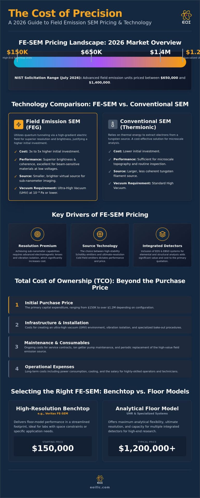
The acquisition of a field emission scanning electron microscope represents a strategic commitment to nanometer-scale precision; the cost of field emission sem reflects the sophisticated engineering required to maintain source coherence and beam stability. In the 2026 fiscal environment, the pricing spectrum for these instruments is tiered according to analytical capacity and resolution thresholds. While entry-level benchtop configurations, such as the Veritas FE SEM, may begin near the $150,000 threshold, fully integrated analytical platforms frequently exceed $1,200,000. This pricing variance is largely dictated by the Resolution Premium, a technical metric that correlates sub-nanometer imaging capabilities with the capital investment required for advanced electromagnetic lens stability and vibration isolation.
Recent procurement data from federal institutions highlights the current market valuation for high-performance systems. For instance, a July 2026 solicitation from the National Institute of Standards and Technology (NIST) indicates a price range of $650,000 to $1,400,000 for advanced field emission units. A notable trend in this cycle is the inclusion of Energy Dispersive Spectroscopy (EDS) and Electron Backscattered Diffraction (EBSD) detectors within the primary system quotation. Manufacturers are increasingly positioning these as integrated solutions rather than modular add-ons to increase the immediate return on investment for industrial research facilities.
To further enhance this return on investment, many laboratories choose to hire auxiliary technical tools rather than purchasing them outright. Partnering with a specialist like Zenith Rental for advanced electrical and industrial testing equipment ensures that the facility remains at the cutting edge of performance while preserving capital for primary imaging systems.
The Physics of Value: Quantum Tunneling vs. Heat
The technical superiority of a Field Emission Gun (FEG) stems from its method of electron extraction. Unlike thermionic sources that rely on thermal energy to overcome the work function of tungsten, FEG systems utilize high-gradient electric fields. Quantum tunneling acts as the fundamental physical mechanism that enables electrons to bypass the potential barrier of the emitter tip, resulting in a significantly smaller and brighter virtual source compared to traditional thermal extraction. This process necessitates an ultra-high vacuum (UHV) environment, typically maintained at 10^-8 Pa or lower, to prevent tip contamination. The infrastructure required for UHV, including ion getter pumps and specialized bake-out procedures, contributes substantially to the total system valuation.
FE-SEM vs. Conventional SEM: A Cost-Benefit Preview
Budgetary planning for the cost of field emission sem must account for an initial investment delta that is typically 3x to 5x higher than conventional tungsten models. This expenditure is justified by the superior brightness and coherence of the electron beam, which remains focused even at low accelerating voltages. Such performance is critical for imaging beam-sensitive polymers or observing topographically complex nanostructures with an extended depth of field. Understanding these technical nuances is essential for laboratory managers who must align their equipment capabilities with specific research objectives, as detailed in our guide on The Fundamental Principles of Scanning Electron Microscopy (SEM) in 2026. It’s clear that while the entry price is higher, the reduction in cost-per-image through enhanced resolution and faster data acquisition provides a compelling long-term economic case for a Scanning Electron Microscope (SEM) featuring field emission technology.
Key Drivers of FE-SEM Pricing: Technology and Configuration
The cost of field emission sem is fundamentally a reflection of the instrument’s ability to maintain high beam brightness and spatial coherence under rigorous analytical conditions. While a standard thermionic source is often sufficient for microscale topography, the transition to field emission technology is necessitated by the pursuit of sub-nanometer resolution and high-speed data acquisition. In 2026, the configuration of the electron optical column and the integration of specialized detectors represent the most significant variables in a final project quote. For organizations operating at the 2nm semiconductor node or developing advanced energy storage materials, the investment is defined by the requirement for a virtual source size that remains stable over extended periods.
Modern pricing structures also reflect the increasing role of automation and artificial intelligence in microscopy workflows. Software suites capable of automated particle analysis or large-area montaging can increase the system’s valuation, yet they provide a measurable increase in laboratory ROI by reducing manual operator time. The final quote is typically influenced by several core components:
- Source Brightness: FE sources provide up to 1,000 times the brightness of tungsten, enabling faster mapping and superior image quality at low accelerating voltages.
- Detector Arrays: The inclusion of high-sensitivity Backscattered Electron (BSE) and Secondary Electron (SE) detectors, alongside integrated EDS for elemental mapping.
- System Footprint: A shift toward high-performance benchtop systems allows facilities to capture floor-model resolution within a smaller, more cost-effective laboratory footprint.
The Brightness Advantage and Analytical Throughput
High brightness isn’t merely a metric of image clarity; it’s a driver of analytical velocity. Increased beam current at small spot sizes allows for rapid Energy Dispersive Spectroscopy (EDS) mapping without the drift associated with longer scan times. This stability is critical for maintaining accuracy during complex characterization sessions. For a deeper technical exploration of these capabilities, consult our resource on Advanced SEM Techniques: A Comprehensive Guide to High-Resolution Analytical Microscopy in 2026.
Chamber Size and Sample Handling
The physical dimensions of the specimen chamber and the complexity of the motorized stage significantly impact the cost of field emission sem. Large-chamber systems designed for 200mm semiconductor wafers or heavy industrial components require sophisticated vibration isolation and multi-axis movement. Conversely, labs focusing on small-scale morphology can find exceptional value in compact configurations. You can compare these different architectural tiers in our guide on How Much Does an Electron Microscope Cost? A Comprehensive 2026 Price Guide. If your research demands nanometer-scale precision within a constrained space, exploring the Veritas FE SEM may provide the ideal balance of performance and logistical efficiency.
Source Technology: Cold Field Emission vs. Schottky Emitters
The cost of field emission sem is fundamentally predicated on the electron extraction mechanism housed within the gun chamber. Buyers must choose between Schottky emitters, also known as thermal field emission, and cold field emission (CFE) sources. This choice dictates not only the initial capital outlay but also the long-term operational rhythm of the laboratory. While both technologies provide the high brightness necessary for nanoscale characterization, they cater to different analytical priorities. Schottky sources remain the industry standard for stability, whereas CFE is reserved for applications requiring the absolute limits of spatial resolution.
Maintenance budgets must account for the replacement cycle of these high-performance sources. Unlike tungsten filaments that may last only weeks, field emission sources typically provide one to three years of service life, depending on vacuum quality and usage patterns. The cost of a replacement FE source can exceed $50,000, making preventative maintenance of the vacuum system a critical fiscal priority. Furthermore, the operational complexity of CFE systems includes the necessity of daily or twice-daily “flashing,” a process that restores tip performance but introduces periodic downtime into the analytical workflow.
Schottky Emitters: The Standard for Modern Lab ROI
Schottky technology utilizes a zirconiated tungsten tip that operates at elevated temperatures to facilitate electron emission. This thermal assistance ensures a highly stable beam current over many hours, which is essential for quantitative Energy Dispersive Spectroscopy (EDS) and automated mapping. The Veritas FE SEM adopts this configuration to provide a reliable, high-resolution platform for multi-user environments where consistent performance is paramount. Over a five-year horizon, Schottky emitters often present a more favorable ROI because they require less frequent intervention and operate under slightly less stringent vacuum conditions than their cold field counterparts.
Cold Field Emission: Pushing the Resolution Frontier
For laboratories engaged in cutting-edge semiconductor research or advanced nanomaterials, the $100,000 premium for CFE technology may be a necessary investment. These systems require extreme vacuum levels, often reaching 10^-9 Pa, to prevent gas molecules from adhering to the sharp emitter tip. CFE achieves sub-1nm resolution by minimizing the energy spread of the emitted electrons, which reduces chromatic aberration in the final probe. Despite this performance advantage, the increased cost of field emission sem systems utilizing CFE must be weighed against the higher technical burden placed on the operator to maintain peak emission levels throughout the day.
Total Cost of Ownership (TCO): Beyond the Initial Purchase
The strategic valuation of a high-resolution imaging platform extends far beyond the procurement invoice. While the initial cost of field emission sem systems represents a significant capital expenditure, successful laboratory management requires a meticulous understanding of the Total Cost of Ownership (TCO). To track these multifaceted laboratory expenses and avoid the “growth tax” often associated with scaling research operations, many organizations rely on modern accounting platforms like EmLedger. Industry data suggests that ongoing operational expenses, including maintenance, consumables, and service contracts, typically add 10% to 15% to the initial investment annually. It’s a fiscal reality that is particularly acute for field emission technology, where the preservation of the ultra-high vacuum (UHV) environment is paramount to protecting the emitter’s integrity.
A comprehensive TCO roadmap must prioritize the stability of the vacuum architecture. Unlike thermionic systems, FE-SEMs rely on a sophisticated combination of ion getter pumps and turbo-molecular pumps to maintain the necessary 10^-8 Pa thresholds. Failure to maintain these systems leads to source contamination, which can necessitate the premature replacement of the field emission gun. Given that a replacement source frequently exceeds $50,000, specialized service contracts aren’t merely an option; they’re a fundamental component of risk mitigation. Infrastructure requirements also contribute to the long-term budget, though high-performance benchtop systems often mitigate these costs by integrating dampening into a smaller footprint. Critical factors include:
- Vibration Isolation: Active or passive dampening systems to ensure sub-nanometer stability.
- EMI Shielding: Protection against electromagnetic interference that can degrade beam coherence.
- Acoustic Dampening: Minimizing environmental noise in high-traffic industrial facilities.
- Consumable Management: Budgeting for final apertures, scintillator tips, and vacuum seals.
The Criticality of Preventative Maintenance
Scheduled technical interventions are the primary defense against catastrophic system failure. Regular vacuum leak checks and pump servicing ensure the source remains in a pristine state, extending its operational life toward the three-year mark. Facilities that prioritize these visits see a measurable increase in uptime and data consistency. For a detailed breakdown of these protocols, refer to The Definitive Guide to SEM Maintenance: Maximizing Precision and Longevity in 2026.
On-Site Training and Technical Support
The human element of the cost of field emission sem is frequently overlooked. Operator error is a leading cause of vacuum compromise and mechanical stage damage. Investing in expert-led training ensures that staff can leverage advanced features, such as automated failure analysis, without risking hardware damage. Customized training programs are particularly valuable for labs specializing in semiconductor inspection or complex metallurgy. You can explore professional operational standards in SEM Operation: The Professional Guide to Scanning Electron Microscopy in 2026. To ensure your facility maintains peak analytical performance, consider scheduling Preventative Maintenance Visits with a certified technician.
Selecting the Right FE-SEM: Benchtop vs. Floor Models
The final stage of strategic procurement involves a critical evaluation of the physical architecture required to meet research objectives. While traditional floor-standing models were once the only pathway to nanometer-scale precision, the rise of the benchtop FE-SEM has introduced a significant paradigm shift in laboratory planning. These compact systems achieve resolution levels that rival their larger counterparts, yet they do so with a significantly reduced footprint. Choosing the correct platform requires a balance between the cost of field emission sem and the physical constraints of the facility, as well as the specific dimensions of the samples being analyzed.
Floor-standing models remain a non-negotiable requirement for facilities processing large-scale specimens, such as 300mm semiconductor wafers or heavy metallurgical components. These systems provide the internal volume necessary for expansive motorized stages and the integration of multiple specialized detectors, including WDS or cryo-transfer suites. However, for organizations focused on high-throughput quality control or routine nanomaterial characterization, the benchtop format offers a more agile investment. Strategic procurement should prioritize vendors who demonstrate localized technical expertise and a proven history of logistical excellence in the US market.
Maximizing ROI with the Veritas FE SEM
The Veritas FE SEM bridges the gap between desktop convenience and the rigorous resolution standards of high-end industrial research. One of the primary drivers of its high ROI is the reduction in infrastructure requirements. Unlike floor models that often necessitate dedicated rooms with reinforced flooring and specialized electromagnetic shielding, the Veritas series operates effectively in standard laboratory environments. It’s the preferred choice for B2B manufacturing and QC environments where analytical throughput must be achieved without the cost of field emission sem facility overhauls. This efficiency allows laboratories to redirect capital toward advanced detector integration or expanded service coverage.
Final Considerations for Your SEM Investment
Before finalizing a purchase, it’s essential to conduct a needs-based analysis of your resolution requirements. While the pursuit of sub-1nm imaging is a common goal, many industrial applications find peak efficiency at slightly higher thresholds where beam stability and ease of use are more critical than absolute magnification. A technical consultation is a vital step in this process, ensuring that the selected configuration aligns with the practical realities of your daily workflow. To ensure your investment delivers the precision your industry demands, Contact Electron Optics Instruments, LLC for a technical consultation on FE-SEM pricing and solutions. Our team provides the expert guidance necessary to navigate the complexities of modern electron optics and long-term system performance.
Optimizing Your Laboratory’s Analytical Future
Transitioning to sub-nanometer resolution requires a meticulous alignment of capital resources with specific technical requirements. The cost of field emission sem systems in 2026 is ultimately defined by the immense gains in beam brightness and analytical throughput that Schottky and Cold Field sources provide for high-precision environments. By prioritizing a comprehensive Total Cost of Ownership model that accounts for ultra-high vacuum stability and preventative maintenance, facilities can effectively protect their investment against the risks of source degradation. It’s a strategic necessity to partner with a seasoned innovator that understands the practical realities of international production and technical integration.
Electron Optics Instruments leverages over 30 years of industry experience as the sole US distributor for EmCraft Scanning Electron Microscopes to deliver sophisticated high-resolution solutions like the Veritas FE SEM. Our expert-driven narrative focuses on providing multi-tiered service contracts and professional on-site training to ensure your hardware maintains its superior standards throughout its operational lifecycle. We invite you to Explore the Veritas FE SEM and High-Resolution Solutions to establish a visionary foundation for your next decade of nanoscale innovation. Your laboratory’s pursuit of accuracy is supported by our established commitment to technical excellence and logistical reliability.
Frequently Asked Questions
What is the main advantage of a field emission scanning electron microscope over a tungsten SEM?
A field emission scanning electron microscope provides up to 1,000 times the brightness and significantly higher spatial coherence compared to a tungsten SEM. This enables sub-nanometer resolution and superior image quality at low accelerating voltages, which is vital for imaging beam-sensitive samples. While the cost of field emission sem technology is higher, it allows laboratories to observe topographical details that are entirely invisible to thermionic systems.
How much more does an FE-SEM cost compared to a standard benchtop SEM?
An FE-SEM typically requires a capital investment that is three to five times greater than a standard tungsten-based benchtop SEM. While entry-level desktop units often range from $60,000 to $150,000, high-resolution field emission configurations generally start at $150,000 and can exceed $1,200,000 for floor-standing analytical platforms. This premium reflects the sophisticated vacuum systems and electromagnetic lens stability required for nanometer-scale precision.
How often does a field emission source need to be replaced?
Field emission sources generally provide a service life of one to three years, which is significantly longer than the few weeks offered by tungsten filaments. The actual longevity depends on the consistency of the ultra-high vacuum and the frequency of system use. Protecting this investment requires rigorous adherence to preventative maintenance protocols to prevent source contamination or mechanical failure during high-precision analytical sessions.
What are the hidden costs of owning a field emission SEM?
The primary hidden expenses include the maintenance of ultra-high vacuum (UHV) components, such as ion getter pumps, and the necessity of specialized service contracts. Infrastructure upgrades for vibration isolation, acoustic dampening, and electromagnetic interference (EMI) shielding can also add substantial figures to the total project budget. Operators must also account for ongoing consumables like final apertures and scintillator tips.
Does an FE-SEM require a specialized room for installation?
Large floor-standing FE-SEMs usually require a dedicated, climate-controlled room with reinforced flooring to mitigate environmental interference. However, advanced benchtop systems like the Veritas FE SEM are engineered to operate in standard laboratory settings. These compact units integrate internal dampening to achieve high-resolution results without the extensive facility modifications typically associated with the cost of field emission sem acquisition.
What is the difference between Schottky and Cold Field Emission in terms of cost?
Cold Field Emission (CFE) systems typically command a premium of $100,000 or more over Schottky emitters due to their superior energy spread and resolution limits. Schottky emitters are often favored for multi-user facilities because they offer better beam stability for long analytical sessions. CFE sources require more frequent technical intervention, such as daily flashing, which increases the operational complexity and potential downtime.
Is it possible to upgrade a conventional SEM to a field emission source?
Upgrading a conventional thermionic SEM to a field emission source is generally not technically or economically feasible. The transition requires a fundamental redesign of the electron optical column and the vacuum architecture to support the 10^-8 Pa thresholds necessary for FEG stability. Most organizations find that the most cost-effective path to field emission capability is the procurement of a purpose-built system like the Veritas series.
What is the typical resolution limit for a modern FE-SEM in 2026?
Modern FE-SEM systems in 2026 typically achieve resolution limits in the sub-nanometer range, often reaching 0.8nm to 1.2nm at optimal accelerating voltages. High-performance configurations can maintain this precision even at low voltages, which is essential for the inspection of next-generation semiconductors and advanced polymers. This capability ensures that laboratories remain competitive in specialized industrial sectors requiring meticulous morphological characterization.