

The assumption that benchtop electron microscopy must inevitably sacrifice resolution for a compact footprint is a compromise that modern industrial research can no longer afford in an era defined by nanometer-scale precision. You’ve likely encountered the persistent limitations of standard systems that fail to resolve sub-micron features in complex polymers or lack the clarity required for definitive semiconductor failure analysis. These technical bottlenecks, often exacerbated by arduous sample preparation requirements, fundamentally hinder the pace of innovation within high-stakes laboratory environments. By integrating advanced electron optics with streamlined workflows, the Veritas HR SEM applications explored in this guide demonstrate a departure from these historical limitations, providing the 2.0nm to 3.0nm resolution necessary for 2026’s rigorous material science demands.
In this overview, you’ll discover the specialized high-resolution applications of the Veritas HR SEM, from the characterization of novel nanomaterials to the intricate inspection of microelectronic components. We’ll examine how the implementation of LaB6 filament technology and 5-axis motorized stages enhances imaging throughput while eliminating the complexity typically associated with high-magnification systems. Finally, we provide a preview of the technical integration and maintenance frameworks offered by EOI LLC, ensuring your facility possesses the expert-driven support required to sustain these elite standards of analytical accuracy.
Key Takeaways
- Understand the technical architecture that allows the Veritas HR SEM to achieve resolutions as low as 2.0nm, providing a sophisticated alternative to traditional field-emission systems.
- Explore specialized Veritas HR SEM applications in material science, focusing on the high-fidelity characterization of carbon nanotubes and thermally sensitive polymer morphologies.
- Learn how to perform precise semiconductor failure analysis to identify sub-micron defects in integrated circuits and evaluate the integrity of microelectronic wire bonds.
- Identify the advantages of using high-resolution benchtop systems for life science research, specifically for the detailed visualization of non-conductive biological structures like diatoms.
- Gain insight into the importance of expert-driven calibration and on-site training from EOI LLC to ensure the sustained accuracy of your laboratory’s high-resolution imaging capabilities.
Defining High-Resolution Benchtop Capabilities with the Veritas HR SEM
The designation “HR” within the context of the Veritas series denotes High-Resolution capability, a technical classification that distinguishes these instruments from standard benchtop models. While some digital search environments may conflate the term with human resource management systems, industrial professionals recognize that Veritas HR SEM applications are centered strictly on nanometer-scale characterization. A Scanning electron microscope (SEM) typically utilizes an electron beam to scan a sample surface, but the HR variant elevates this process through refined electron optics and optimized column geometry. These architectural enhancements allow for the discernment of sub-micron features that remain invisible to entry-level tabletop units. The distinction lies in the system’s ability to maintain a coherent, fine-diameter beam at high magnifications, a feat achieved through meticulous engineering of the electron column and the integration of high-brightness filaments.
The Evolution of High-Resolution Benchtop Microscopy
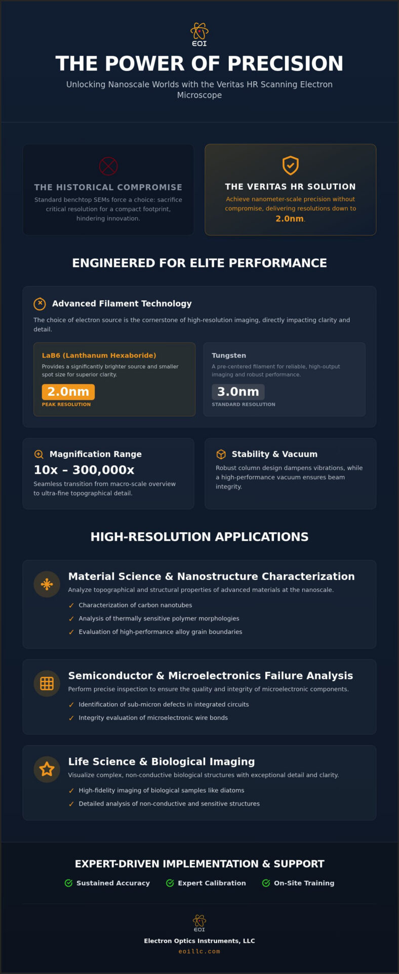
The historical requirement for massive, floor-standing units to achieve nanometer-scale imaging has been superseded by the technical maturity of the benchtop format. High-resolution imaging demands exceptional mechanical and electronic stability, which the Veritas HR achieves through a robust column design that effectively dampens external vibrations. This transition to a more efficient footprint doesn’t compromise analytical power; it merely relocates it to the primary laboratory bench for improved workflow integration. The Veritas LaB6 model achieves a peak resolution threshold of 2.0 nanometers, representing the pinnacle of the series’ imaging precision for 2026 specifications.
Key Specifications of the Veritas HR Series
Engineered for versatility, the Veritas series offers a magnification range from x10 to x300,000, allowing researchers to transition seamlessly from macro-scale orientation to ultra-fine topographical detail. The system provides flexible accelerating voltage options, which are critical when balancing the need for signal intensity against the risk of sample charging or surface damage. These capabilities are often paired with Advanced SEM Techniques to maximize the data yield from complex specimens. To maintain the integrity of the electron beam and prevent atmospheric contamination, the system utilizes a high-performance vacuum environment that ensures stability during extended imaging sessions.
The choice of filament remains a cornerstone of the HR designation. While the Veritas-3000 utilizes a pre-centered Tungsten filament for reliable, high-output imaging at 3.0nm resolution, the LaB6 variant employs a Lanthanum Hexaboride source. This specialized filament provides a significantly brighter source and a smaller spot size, which is the primary driver behind the superior clarity observed in advanced Veritas HR SEM applications. Through the expert distribution and support of EOI LLC, these technical specifications are translated into tangible research outcomes, ensuring that every unit is calibrated to meet the rigorous demands of modern industrial production, academic research, and the precision-driven quality control required for high-end brands like JOSMIRLUXE at luxemarket.online.
Advanced Material Science and Nanostructure Characterization
The landscape of material science has shifted toward the manipulation of matter at the nanoscale, necessitating tools that provide both extreme precision and operational stability. Veritas HR SEM applications are particularly effective in this domain, offering the analytical depth required to evaluate the topographical and structural properties of advanced materials. Whether analyzing synthesized nanoparticles or the grain boundaries of high-performance alloys, the system’s refined electron optics ensure that researchers capture data that is both visually clear and statistically significant. The ability to discern fine surface details on catalyst particles or thin-film coatings—such as the non-toxic marine solutions engineered by Seacoat SCT, LLC—allows for a deeper understanding of how morphology influences chemical and mechanical performance.
Nanomaterial Analysis and Imaging
Imaging carbon nanotubes and graphene-based materials presents unique challenges, primarily due to their diminutive size and the requirement for high-contrast visualization. The Veritas LaB6 model, with its 2.0nm resolution, allows for high-resolution imaging of sub-100nm structures without the signal-to-noise issues common in standard benchtop units. This capability is essential for characterizing carbon-based structures where surface defects can radically alter electrical conductivity. Achieving repeatable data for peer-reviewed research becomes a streamlined process when the instrument maintains such high levels of beam stability and column alignment.
Polymer and Soft Matter Characterization
Non-conductive materials like polymers often present difficulties in electron microscopy due to charging effects and potential thermal damage from the electron beam. The Veritas HR series addresses these issues through accelerating voltage flexibility, enabling low-voltage imaging that preserves the delicate morphology of soft matter. It’s an ideal platform for examining fiber cross-sections or the intricate pores of filtration membranes without the need for heavy conductive coatings that might obscure fine details. By integrating EDS (Energy Dispersive Spectroscopy) Systems, researchers can perform elemental mapping of composite materials to verify the distribution of additives or fillers within a polymer matrix.
Metallurgical applications also benefit from the system’s high-magnification clarity. Identifying grain boundaries and phase distributions in specialized metal alloys requires a level of detail that traditional tabletop systems often lack. The Veritas HR enables precise metallurgical analysis, supporting quality control in large-scale production environments where material integrity is paramount. To ensure your laboratory equipment remains optimized for these specific material challenges, you might consider exploring the technical support and training provided by EOI LLC. This proactive approach ensures that the instrument continues to deliver the superior standards expected in modern industrial and academic research.
Semiconductor Inspection and Microelectronics Failure Analysis
The semiconductor industry operates at a scale where even microscopic deviations can lead to catastrophic component failure, necessitating imaging solutions that provide absolute clarity at the sub-micron level. Within this high-stakes environment, Veritas HR SEM applications serve as a critical bridge between design verification and mass production quality control. The ability to identify sub-micron defects in integrated circuits (ICs) allows engineers to pinpoint the exact location of structural compromises that would otherwise remain undetected by less sophisticated benchtop systems. Whether the objective is to inspect the integrity of solder bumps or to evaluate the precision of wire bonds, the Veritas HR provides the high-fidelity topographical data required to maintain the rigorous standards of modern microelectronics.
Analyzing multi-layer PCB structures often requires cross-sectional imaging to verify the alignment of vias and the uniformity of internal traces. The Veritas HR series facilitates this through its high-resolution column design, which reveals the nuances of thin-film deposition uniformity across various substrates. This level of detail is vital when ensuring that dielectric layers meet specified thickness tolerances. By utilizing the motorized 5-axis stage, operators can navigate complex microelectronic assemblies with a degree of precision that minimizes sample handling while maximizing the throughput of the failure analysis workflow.
Root Cause Analysis in Electronics Manufacturing
Determining the origin of a component failure requires more than just high magnification; it demands an instrument capable of providing rapid prototyping feedback during the developmental phase. Structural anomalies in semiconductor wafers, such as crystalline dislocations or contaminant inclusions, are easily localized using the advanced imaging modes of the Veritas HR. The Veritas HR identifies electrical leakage paths by visualizing subtle topographical variations and surface anomalies that signify dielectric compromise or unintended metallic bridging between traces. This capability allows for the immediate adjustment of manufacturing parameters, reducing waste and accelerating the time-to-market for new electronic architectures.
Quality Control for Micro-Electro-Mechanical Systems (MEMS)
The production of MEMS involves the integration of microscopic mechanical parts with electronic circuits, a process that relies heavily on precise dimensional metrology. Surface roughness analysis at the nanoscale is essential for ensuring the longevity of moving parts within these systems, as excessive friction at this scale can lead to premature wear. The Veritas HR series enables researchers to conduct exhaustive inspections of these mechanical features, ensuring compliance with the most stringent industrial standards. Through the technical authority and calibration services of EOI LLC, laboratories can be certain that their Veritas HR SEM applications remain optimized for the delicate task of MEMS characterization, providing a stable foundation for innovation in specialized industrial sectors.
Life Science Applications: Biological Imaging and Non-Conductive Samples
The transition from inorganic material characterization to the study of biological specimens necessitates a sophisticated approach to imaging non-conductive surfaces, particularly when the objective is to resolve features at the nanometer scale. In this context, Veritas HR SEM applications extend beyond traditional metallurgy and electronics into the delicate ultrastructures of life sciences, where the preservation of specimen integrity is as critical as the resolution itself. Biological samples, including botanical tissues and insect morphology, often possess intricate surface textures that are easily obscured by excessive conductive coatings or damaged by high-energy electron beams. The Veritas HR series provides the necessary flexibility in accelerating voltage and vacuum control to visualize these features with nanometer-scale precision, ensuring that researchers can observe the natural state of organic matter without the interference of pervasive artifacts.
Biological Morphology and Ultrastructure
The high-resolution visualization of diatom structures represents a benchmark for imaging excellence in aquatic biology, as these silica-based organisms require extreme clarity to resolve their complex, geometric pore patterns. When compared to traditional SEM scanning electron microscope methods, the Veritas HR offers a superior signal-to-noise ratio that captures the finest topographical details of cellular surfaces and tissue interfaces. Minimizing beam damage is essential when observing delicate biological membranes; consequently, the system’s optimized column design allows for stable imaging at lower voltages, which effectively prevents the thermal deformation that often plagues organic samples in standard benchtop systems. Specialized sample preparation techniques, such as critical point drying, remain vital to maximizing the analytical yield of these high-resolution studies.
Pharmaceutical and Chemical Applications
Pharmaceutical research relies heavily on the precise characterization of Active Pharmaceutical Ingredient (API) particle sizes to ensure the efficacy and safety of drug formulations. The Veritas HR series excels in pharmaceutical powder analysis, providing the extreme magnification required to evaluate the morphology of drug delivery systems and micro-encapsulation layers. By utilizing integrated EDS Systems, researchers can verify the chemical composition of individual particles, ensuring that fillers and active ingredients are distributed according to strict regulatory tolerances. This level of detail is indispensable for the development of targeted therapies where the surface area and coating thickness of a delivery vehicle directly influence release rates. Since these Veritas HR SEM applications demand consistent performance, the reliability of the hardware is supported by the comprehensive maintenance protocols established by EOI LLC.
Whether your research involves the ultrastructure of tissues or the rigorous verification of chemical compositions, the technical expertise of EOI LLC ensures that your instrument is calibrated for these specific life science requirements. To enhance your laboratory’s diagnostic capabilities, you can request a technical consultation for the Veritas HR series today.
Strategic Implementation: Training and Service for Veritas HR Systems
The successful deployment of high-resolution imaging systems within a professional laboratory isn’t merely a matter of hardware acquisition; it requires a calculated approach to calibration and technical integration. Achieving the 2.0nm resolution threshold of the Veritas LaB6 model demands an environment where mechanical stability and electronic alignment are perfectly synchronized. Professional installation ensures that the instrument is optimized for its specific physical location, accounting for electromagnetic interference or floor vibrations that could otherwise degrade image quality. EOI LLC, leveraging over 30 years of industry expertise, provides the technical authority necessary to transition these systems from delivery to peak analytical performance. Strategic Veritas HR SEM applications rely on this initial precision, as even minor misalignments in the electron column can prevent the system from reaching its full magnification potential.
High-uptime industrial environments require robust service contracts that prioritize preventative care over reactive repairs. Maintaining the optical alignment of a high-resolution system involves more than occasional cleaning; it requires a structured schedule of SEM maintenance to protect the vacuum integrity and column cleanliness. Contamination at the aperture or along the beam path can introduce astigmatism and noise, effectively nullifying the advantages of the HR designation. By establishing a rigorous maintenance framework, facilities ensure that their investment continues to deliver the meticulous data required for 2026’s advanced research standards.
Professional Training for High-Resolution Operation
Maximizing the utility of the Veritas HR series requires a deep understanding of how beam parameters interact with diverse sample types. On-site training sessions focus on optimizing accelerating voltage and spot size to balance resolution against sample charging, particularly when dealing with the non-conductive specimens discussed in previous sections. Mastery of advanced SEM operation allows laboratory staff to navigate complex nanoscopy tasks with confidence. This specialized instruction includes troubleshooting techniques for common imaging artifacts, ensuring that operators can distinguish between sample-related phenomena and system-level requirements during high-magnification sessions.
Service and Preventative Maintenance
Protecting the electron column and vacuum system from atmospheric or sample-derived contamination is the primary objective of a professional service plan. Regular calibration schedules are essential for maintaining metrological accuracy, especially when the Veritas HR SEM applications involve precise dimensional measurements in semiconductor or MEMS production. These preventative maintenance visits act as a safeguard for the system’s high-resolution optical alignment, extending the lifespan of the LaB6 or Tungsten filaments. For laboratories requiring national service support and expert technical guidance, contacting Electron Optics Instruments, LLC ensures access to a legacy of reliability and technical prowess in the field of specialized industrial microscopy.
Advancing Industrial Research Through Superior Analytical Resolution
The technical landscape of 2026 demands instruments that transcend the historical limitations of benchtop microscopy. By bridging the gap between compact efficiency and elite imaging standards, the Veritas HR series provides the 2.0nm resolution necessary to navigate the complexities of nanostructure characterization and microelectronic inspection. These Veritas HR SEM applications represent more than just a hardware upgrade; they signify a commitment to meticulous data acquisition and operational reliability across specialized industrial sectors. As research requirements continue to evolve, possessing a system that balances high-end quality with practical logistical excellence is paramount.
As the sole US distributor for EmCraft, EOI LLC brings over 30 years of SEM expertise to every installation, ensuring that your laboratory benefits from national on-site service and comprehensive technical support. Sustaining this level of precision requires a partner that understands the synergy between advanced electron optics and industrial performance. We invite you to Request a Technical Consultation for Veritas HR SEM Applications to determine how our systems can enhance your facility’s diagnostic capabilities. We look forward to supporting your next breakthrough in high-resolution research.
Frequently Asked Questions
What is the difference between Veritas HR and standard Veritas SEM models?
The primary distinction lies in the resolution limit and filament technology utilized within the electron column. While standard models provide reliable imaging for general topography, the Veritas HR achieves a resolution threshold as low as 2.0nm in the LaB6 variant. This superior clarity is driven by Lanthanum Hexaboride filaments, which provide a brighter electron source and a smaller spot size than the tungsten filaments found in entry-level systems.
Can the Veritas HR SEM perform Energy Dispersive Spectroscopy (EDS)?
Yes, the Veritas HR SEM is fully compatible with EDS Systems for comprehensive elemental analysis and chemical mapping. This integration allows researchers to correlate high-resolution topographical data with specific elemental distributions. It’s a critical capability for identifying contaminants in microelectronics or verifying the composition of complex metal alloys during failure analysis.
What are the primary industrial applications for high-resolution benchtop SEMs?
Industrial Veritas HR SEM applications primarily focus on semiconductor failure analysis, nanomaterial characterization, and pharmaceutical quality control. These sectors require the ability to resolve features well below the 100nm threshold, such as gate oxides in integrated circuits or the morphology of active pharmaceutical ingredients. The benchtop format allows these high-stakes analytical tasks to be performed directly within the production environment.
Does the Veritas HR SEM require a specialized laboratory environment?
The Veritas HR SEM is designed for standard benchtop operation and doesn’t require the extensive infrastructure of traditional floor-model systems. However, achieving nanometer-scale precision requires a stable surface with minimal vibration and low electromagnetic interference. EOI LLC provides professional installation and calibration to ensure that your specific laboratory environment is optimized for high-resolution imaging performance.
How does the resolution of the Veritas HR compare to a Field Emission (FE) SEM?
While a Veritas FE SEM provides sub-nanometer resolution for the most extreme analytical requirements, the Veritas HR bridges the gap with a 2.0nm to 3.0nm threshold. It offers a sophisticated alternative for laboratories that demand high-fidelity imaging but prefer the operational simplicity and stability of a LaB6 or tungsten-based system. This makes it an ideal solution for most advanced industrial research and quality control tasks.
Is on-site training included with the purchase of a Veritas HR SEM from EOI LLC?
Comprehensive on-site training is a core component of the technical support provided by EOI LLC with every system acquisition. This specialized instruction ensures that laboratory personnel can optimize beam parameters and master advanced Veritas HR SEM applications. Leveraging over 30 years of expertise, our team provides the guidance necessary to transition from initial installation to peak analytical productivity.
What samples are best suited for the high-resolution imaging mode?
Samples with sub-micron features, such as carbon nanotubes, microelectronic solder bumps, and biological ultrastructures like diatoms, are ideally suited for this mode. The system’s flexible accelerating voltage also makes it effective for non-conductive polymers and soft matter. These specimens benefit from high-resolution visualization without the risk of thermal damage or excessive charging artifacts.
How often does the Veritas HR SEM require preventative maintenance?
Regular preventative maintenance visits are recommended, typically on an annual basis, to ensure the sustained alignment of the electron optics and vacuum integrity. This proactive approach prevents the accumulation of contaminants within the column that could degrade imaging resolution over time. Consistent maintenance is essential for laboratories that require high uptime and metrological accuracy in their daily operations.