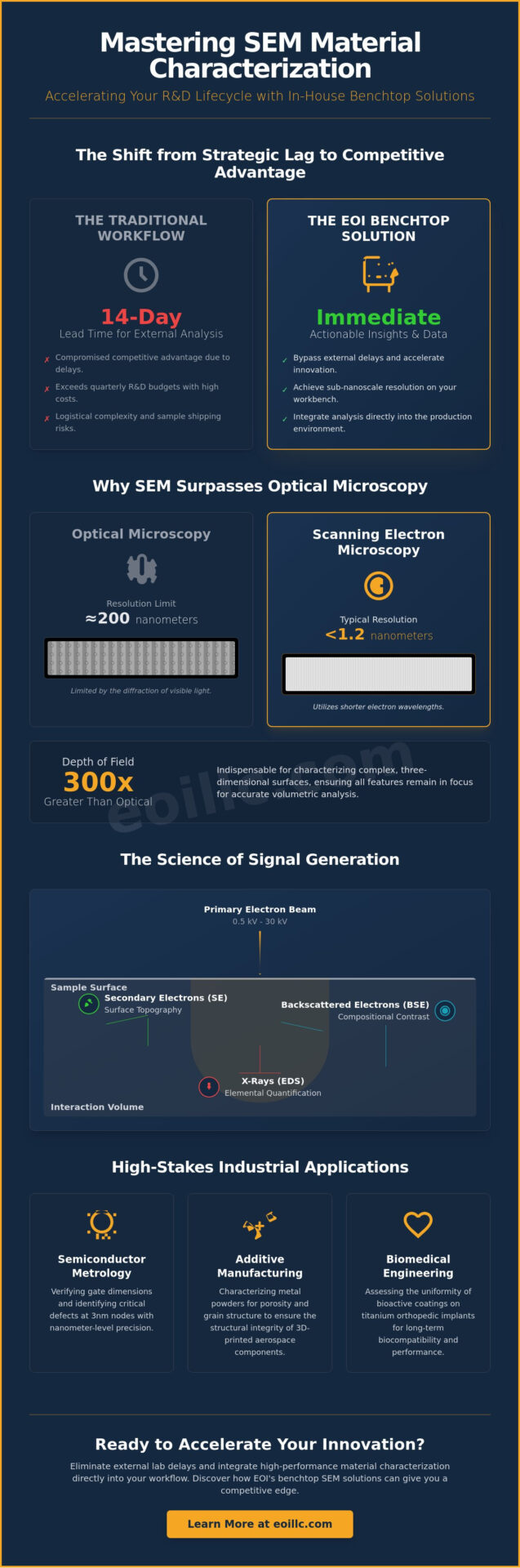
What if the primary bottleneck in your 2026 product development cycle isn’t a lack of data, but the 14-day lead time required for external sem material characterization? As the industry pivots toward advanced nanomaterials that require precision at the 1.2 nanometer level, the traditional reliance on centralized microscopy cores often results in a strategic lag that compromises competitive advantage. You likely recognize that achieving sub-nanoscale resolution is no longer a luxury but a fundamental requirement for industrial innovation and global manufacturing excellence.
It’s frustrating when complex electron-matter interactions lead to ambiguous results or when external testing costs exceed your quarterly R&D budget. You deserve a workflow that provides immediate, actionable insights into your material’s morphological and elemental properties. This guide empowers you to master these complexities, offering a clear framework for differentiating between SE and BSE signals while optimizing EDS for precise quantification. We’ll examine how the evolution of high-resolution benchtop SEM technology allows your team to bypass external delays, ensuring your analytical capabilities align with the rigorous standards of modern engineering.
Key Takeaways
- Identify the strategic transition from qualitative imaging to quantitative analytical microscopy to ensure precision within the modern product lifecycle.
- Analyze the physics of electron-matter interactions to optimize beam energy settings for superior resolution and penetration depth control.
- Master the integration of Energy Dispersive Spectroscopy (EDS) for the accurate elemental quantification of complex multi-component systems.
- Establish a methodical framework for sem material characterization that adapts accelerating voltage and vacuum parameters to specific sample conductivities.
- Accelerate industrial innovation by deploying automated benchtop solutions that streamline particle sizing and grain analysis through sophisticated software integration.
The Evolutionary Role of SEM in Modern Material Characterization
In the sophisticated landscape of 2026 industrial engineering, sem material characterization represents the essential intersection of high-resolution topographic imaging and precise chemical analysis. This methodology employs a focused beam of electrons to interact with the sample surface, generating signals that reveal critical information regarding morphology, composition, and crystallographic structure. As global manufacturing requirements move toward the sub-nanoscale, the role of scanning electron microscopy has evolved from a purely qualitative observation tool into a rigorous quantitative analytical platform. This evolution is particularly vital within the framework of the Materials Genome Initiative, where the rapid iteration of new alloys and polymers demands immediate, high-fidelity data to accelerate the R&D lifecycle.
The industrial landscape has historically relied on massive, floor-model systems that require dedicated facilities and specialized staff. However, the paradigm is shifting. The emergence of high-performance desktop SEM solutions allows organizations to integrate advanced characterization directly into their production environments. This decentralization ensures that precision is maintained without the logistical delays inherent in centralized laboratory testing, fostering a culture of continuous improvement and sustainable innovation. It’s no longer necessary to sacrifice performance for accessibility; modern benchtop systems now deliver the resolution and stability previously reserved for large-scale installations.
Why SEM Surpasses Optical Microscopy for Characterization
The limitations of optical microscopy are primarily dictated by the diffraction limit of visible light, which restricts resolution to approximately 200 nanometers. SEM overcomes this physical barrier by utilizing electrons, which possess significantly shorter wavelengths, allowing for resolution levels frequently exceeding 1.2 nanometers in modern benchtop systems. Additionally, electron optics provide a depth of field approximately 300 times greater than that of light-based systems. This capability is indispensable when characterizing complex, three-dimensional surfaces that require all features to remain in focus simultaneously for accurate volumetric analysis.
Industrial Drivers for Advanced Characterization
The demand for precise sem material characterization is driven by several high-stakes sectors that prioritize excellence and reliability:
- Semiconductor Metrology: As industry standards move toward 3nm nodes, SEM is the only viable method for verifying gate dimensions and identifying defects with nanometer precision.
- Additive Manufacturing: Characterizing metal powders for porosity and grain structure is essential to ensure the structural integrity of 3D-printed aerospace components.
- Biomedical Engineering: Assessing the uniformity of bioactive coatings on titanium orthopedic implants requires the high-contrast imaging capabilities of SEM to ensure long-term biocompatibility and performance.
Electron-Matter Interactions: The Science of Signal Generation
Understanding the physics of signal generation is the cornerstone of sem material characterization. When the primary electron beam strikes a specimen, it creates an interaction volume, a localized region where electrons undergo multiple scattering events. The dimensions of this volume are primarily governed by the accelerating voltage, typically ranging from 0.5 kV to 30 kV. Lower voltages restrict the interaction to the near-surface region, whereas higher voltages facilitate deeper penetration, often reaching depths of five microns or more. Mastering the sem scanning electron microscope working principles is essential for interpreting how these varying depths influence the resulting data.
The signals generated within this volume are categorized by the nature of their scattering mechanisms. Inelastic scattering occurs when the primary beam transfers energy to the sample atoms, resulting in the emission of secondary electrons and X-rays. Conversely, elastic scattering involves the deflection of primary electrons by the atomic nuclei, producing backscattered electrons. It’s vital to recognize that modern 2026 systems often employ variable pressure modes to manage charge-up on non-conductive samples. This capability alters the interaction volume dynamics compared to traditional high-vacuum models, offering a more versatile approach to sem material characterization.
Secondary Electrons (SE) for Topographical Mapping
Secondary electrons are low-energy particles, typically defined as having kinetic energies less than 50 eV. Because of their low energy, only those generated within the initial 5 to 50 nanometers of the sample surface can escape and reach the detector. This surface sensitivity makes SE imaging the primary tool for high-resolution morphological assessment. It excels at highlighting edge effects and fine surface roughness, providing a vivid three-dimensional representation of the specimen’s topography. Secondary electrons are the primary tool for high-resolution morphological assessment.
Backscattered Electrons (BSE) for Compositional Contrast
Backscattered electrons result from elastic collisions and retain a significant portion of the primary beam’s energy. The efficiency of this backscattering is directly proportional to the atomic number (Z) of the material. Heavier elements, such as tungsten (Z=74), appear significantly brighter than lighter elements like aluminum (Z=13). This relationship allows for rapid phase identification and the mapping of elemental distribution within multi-component alloys. While SE signals are usually captured by Everhart-Thornley detectors, BSE signals require dedicated solid-state detectors positioned directly above the sample to maximize capture efficiency. Engineers seeking to optimize their analytical workflows can explore integrated microscopy solutions that streamline the transition between these critical signal modes.
Integrating Energy Dispersive Spectroscopy (EDS) for Elemental Analysis
Energy Dispersive Spectroscopy (EDS) represents the definitive analytical extension of sem material characterization, transforming a purely visual tool into a comprehensive chemical laboratory. This technique functions by measuring the energy and intensity distribution of characteristic X-rays emitted from a specimen during electron bombardment. When the primary electron beam displaces an inner-shell electron, an outer-shell electron fills the vacancy, releasing a photon with an energy signature unique to the specific element. By 2026, the integration of high-throughput Silicon Drift Detectors (SDD) has allowed for collection speeds exceeding 200,000 counts per second, enabling real-time chemical identification that was previously unattainable in benchtop configurations.
The synergy between morphological imaging and elemental spectroscopy is fundamental to advanced sem techniques. Modern systems no longer treat EDS as a secondary attachment; instead, they utilize unified software architectures that overlay chemical data onto high-resolution secondary electron images. This holistic approach allows engineers to move beyond qualitative identification (simply knowing which elements are present) to rigorous quantitative analysis, where the weight percentage of each constituent is calculated with high precision. This capability is vital for verifying alloy specifications or identifying trace contaminants that could compromise the integrity of a global supply chain.
X-Ray Mapping and Line Scans
Spatial distribution of elements is best visualized through color-coded X-ray maps, where each pixel correlates to a specific elemental concentration. Line scans offer a more focused analytical path, providing a graphical representation of elemental fluctuations across a diffusion gradient or a multi-layer interface. It’s important to recognize that while secondary electron imaging achieves nanometer-scale resolution, the lateral resolution of EDS is typically limited to 1 to 3 microns in bulk samples. This discrepancy arises because X-rays are generated from the entire interaction volume rather than just the surface layer.
Quantification Challenges and Standards
Achieving accurate sem material characterization through EDS requires a sophisticated understanding of Matrix (ZAF) corrections. These algorithms account for three critical variables: Atomic number (Z), Absorption (A), and Fluorescence (F). Standardless analysis has become highly reliable for routine screening in 2026, yet standard-based quantification remains the benchmark for industrial excellence in failure analysis. Furthermore, sample geometry plays a decisive role; a tilt of even 10 degrees can significantly alter the X-ray take-off angle, potentially skewing the data if the software does not compensate for the topographical orientation of the specimen.
Strategic Application: Tailoring Parameters for Diverse Material Classes
Precision in sem material characterization is contingent upon the deliberate calibration of electron beam parameters to the specific physical properties of the specimen. For conductive metallic alloys, an accelerating voltage of 15 kV to 25 kV is typically employed to maximize signal-to-noise ratios and facilitate robust X-ray excitation for elemental mapping. Conversely, non-conductive ceramics and biological specimens necessitate a transition to low-vacuum (LV) mode. By introducing a controlled atmosphere of 10 to 130 Pa into the chamber, positive gas ions effectively neutralize surface charging, allowing for artifact-free imaging without the requirement for traditional gold or carbon sputter coating. This strategic flexibility is paramount in failure analysis sem, where preserving the original fracture surface chemistry is critical for accurate root cause determination.
The interplay between beam current and spot size represents a fundamental trade-off that requires a nuanced understanding of electron optics. A larger spot size, achieved through higher beam currents, provides the intense signal required for rapid EDS quantification, yet it inherently degrades lateral resolution. To achieve the nanometer-scale precision required for modern semiconductor metrology, operators must utilize smaller spot sizes and lower currents, often necessitating advanced denoising algorithms to maintain image clarity. Balancing these variables ensures that the analytical output aligns with the rigorous standards of global manufacturing and sustainable innovation.
Characterizing Metals and Ceramics
Metallurgical excellence depends on the clear visualization of grain boundaries and secondary phase distributions. Utilizing high resolution sem allows for the identification of sub-micron precipitates that often dictate the mechanical properties of aerospace-grade alloys. Achieving this level of detail requires rigorous sample preparation, typically involving mechanical polishing to a 0.05-micron finish followed by selective chemical etching to reveal the underlying microstructural architecture. You can optimize your material characterization protocols by integrating these high-resolution workflows into your internal R&D processes.
Polymers, Nanomaterials, and Beam-Sensitive Samples
Characterizing polymers and delicate nanomaterials requires specialized strategies to mitigate beam-induced damage and thermal degradation. Field emission scanning electron microscope sources are particularly advantageous here, as they maintain exceptional brightness even at low accelerating voltages, typically below 1.5 kV. This low-kV approach minimizes electron penetration and heat accumulation, ensuring that the resulting data reflects the true surface morphology rather than structural collapses caused by excessive energy deposition. Utilizing these parameters allows for the precise sem material characterization of photoresists and carbon-based composites without compromising specimen integrity.
The Future of Material Characterization: EOI LLC Benchtop Solutions
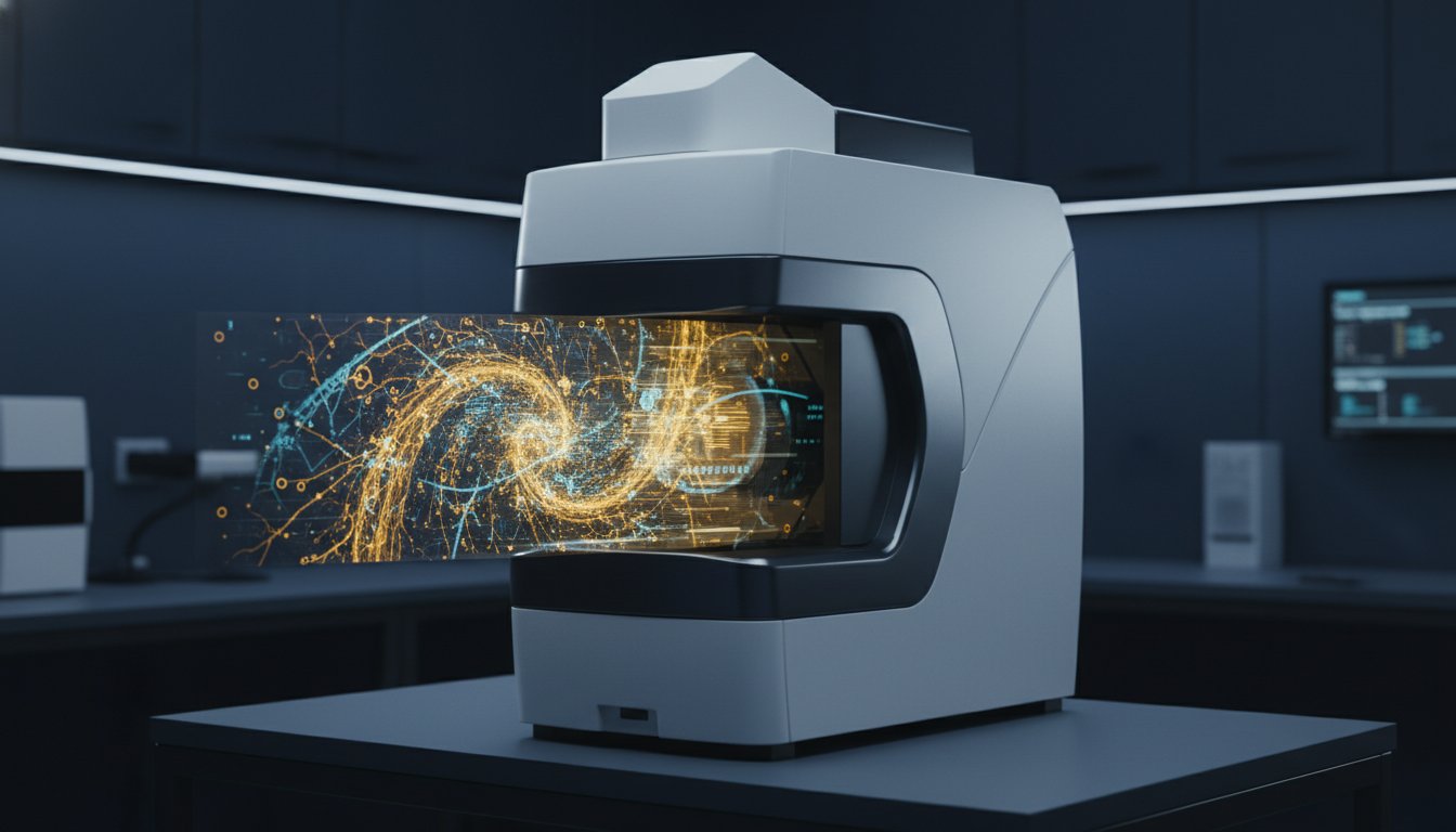
The trajectory of sem material characterization in 2026 is defined by the democratization of high-resolution optics through integrated benchtop platforms. The Cube II Benchtop SEM stands as the pinnacle of this technological shift, offering an accessible yet uncompromising solution for complex industrial analysis. By consolidating high-brightness electron sources and advanced detection systems into a compact footprint, the Cube II enables researchers to achieve sub-5nm resolution without the infrastructure requirements of traditional floor-model systems. This accessibility ensures that precision remains a core component of the localized manufacturing process, facilitating immediate feedback loops in quality control and R&D.
Beyond hardware capabilities, the integration of AI-driven automated software has revolutionized how data is processed. Modern EOI LLC systems utilize sophisticated algorithms for rapid particle sizing and grain analysis, reducing the time required for statistical characterization by up to 70% compared to manual methods. This automation doesn’t just increase throughput; it eliminates the human subjectivity that can compromise the reliability of metallurgical reports. To preserve this analytical accuracy over the long term, rigorous sem maintenance protocols are essential. EOI LLC supports these efforts through comprehensive on-site training and technical support, ensuring your team possesses the expertise to maintain peak operational performance.
From Genesis to Veritas: Scaling Your Characterization Capability
EOI LLC provides a scalable evolutionary path for organizations at every stage of their technical journey. The Genesis Tabletop series offers a robust entry-point for industrial needs, focusing on ease of use and rapid screening of morphological features. For organizations requiring the highest levels of precision, the Veritas HR series delivers research-grade resolution and advanced vacuum control in a compact footprint. Both series allow for customized EDS integration, ensuring that your sem material characterization workflow is tailored to the specific chemical sensitivities of your unique material classes.
The EOI LLC Advantage: Precision, Reliability, and Expertise
Choosing a characterization partner requires a focus on both technical prowess and long-term stability. EOI LLC leverages over 30 years of electron optics experience to provide solutions that balance visionary innovation with the practical realities of global manufacturing. Our comprehensive service contracts are designed to ensure zero-downtime operations, reflecting our commitment to the intersection of reliability and excellence. It’s this dedication to the entire product lifecycle that makes EOI LLC a trusted authority in the optical and automotive sectors. Explore our full range of SEM solutions for material characterization to elevate your analytical capabilities today.
Advancing Industrial Precision Through Analytical Excellence
The path toward industrial leadership in 2026 requires more than just high-resolution imagery. It demands a sophisticated mastery of sem material characterization that bridges the gap between morphological observation and elemental quantification. By integrating advanced EDS workflows with the high-performance capabilities of benchtop systems, organizations achieve a level of precision that drives sustainable innovation and manufacturing excellence. This strategic shift ensures that critical data remains accessible within the production environment, accelerating the R&D lifecycle.
EOI LLC brings over 30 years of electron optics experience to your facility, serving as the sole US distributor for EmCraft Scanning Electron Microscopes. We don’t just provide high-end hardware; we deliver comprehensive on-site technical training and service to ensure your analytical accuracy remains absolute. This holistic approach empowers your team to interpret complex electron-matter interactions with confidence. Take the next step in your analytical evolution by securing the visionary tools necessary for your next breakthrough. Request a Consultation for Your Material Characterization Needs and elevate your laboratory’s capabilities today.
Frequently Asked Questions
What is the primary difference between SEM and EDS in material characterization?
Scanning Electron Microscopy (SEM) provides high-resolution topographic imaging, while Energy Dispersive Spectroscopy (EDS) identifies the specific elemental composition of the sample. While SEM uses secondary or backscattered electrons to map surface features, EDS measures characteristic X-rays to determine chemical identity. This dual approach is fundamental to comprehensive sem material characterization, allowing engineers to correlate physical defects with chemical contaminants.
How does accelerating voltage (kV) affect the quality of material analysis?
Accelerating voltage determines the penetration depth and the size of the interaction volume within the specimen. A higher voltage, such as 20 kV, facilitates deeper penetration and higher X-ray yield but may obscure fine surface details due to a larger interaction zone. Conversely, lower voltages around 1 kV to 5 kV provide superior surface sensitivity, which is critical for observing nanometer-scale features on delicate or low-density materials.
Can SEM be used to characterize non-conductive materials like polymers?
Yes, scanning electron microscopy effectively characterizes non-conductive materials through the use of low-vacuum modes or conductive sputter coatings. In 2026, many benchtop systems utilize charge-reduction modes that introduce a small amount of gas into the chamber to neutralize surface charge. This allows for the direct imaging of polymers and biological samples without the 10-nanometer gold or carbon layers typically required in high-vacuum environments.
What are the benefits of using a benchtop SEM for industrial characterization?
Benchtop systems provide immediate, on-site analytical capabilities that reduce the 7-to-14-day lead times associated with external testing labs. Their compact footprint and automated software allow for a 40% increase in characterization throughput for routine quality control tasks. These systems maintain research-grade resolution, often reaching 1.2 nm, while being accessible to a broader range of engineering staff through intuitive user interfaces.
How often should an SEM be calibrated to ensure accurate material data?
Systems should undergo a basic calibration check every 24 hours of operation to ensure magnification and beam stability remain within specified tolerances. A more comprehensive NIST-traceable calibration for EDS quantification and stage accuracy is recommended every 6 to 12 months. Adhering to these rigorous maintenance cycles is essential for maintaining the integrity of data in a global manufacturing environment.
What is the difference between qualitative and quantitative EDS analysis?
Qualitative EDS identifies which elements are present in a sample by analyzing peak positions, while quantitative EDS calculates the exact weight or atomic percentage of each element. Quantitative analysis requires higher beam stability and often involves ZAF matrix corrections to account for atomic number and absorption effects. In most industrial failure analysis cases, a weight percentage accuracy of 1% to 2% is achievable with proper standardization.
Is sample preparation necessary for all types of SEM material characterization?
While many modern systems offer near-native imaging, most high-precision characterization tasks still require some level of preparation. For metallurgical samples, mechanical polishing to a 0.05-micron finish is standard to reveal grain structures. However, for large-scale topographical screening of fractures, samples can often be placed directly into the chamber, provided they are clean and securely mounted to prevent vibration during imaging.
How do secondary electrons differ from backscattered electrons in imaging?
Secondary electrons (SE) originate from the very surface of the sample and are used primarily for high-resolution topographical imaging. Backscattered electrons (BSE) result from elastic collisions with atomic nuclei deeper in the sample, with their intensity correlating to the atomic number. This allows BSE to provide compositional contrast, where heavier elements appear brighter, making it a critical tool for phase identification during sem material characterization.